- 您现在的位置:买卖IC网 > Sheet目录310 > APEK4402KLP-01-T-DK (Allegro Microsystems Inc)BOARD EVAL FOR A4402
�� �
�
�A4402�
�Constant� On-Time� Buck� Converter�
�With� Integrated� Linear� Regulator�
�Functional� Description�
�?� R1� +� R2� ?�
�V� SW� =� V� FB1� ?� ?�
�,�
�?� (1)�
�V� LIN� =� V� FB2� ?� ?�
�?� R3� +� R4� ?�
�.�
�?�
�R4�
�BasicOperation� TheA4402containsafixedon-time,adjust-�
�able� voltage� buck� switching� regulator� with� valley� sensing� current�
�mode� control,� and� an� adjustable� linear� regulator� designed� to� run�
�off� the� buck� regulator� output.� The� constant� on-time� converter�
�maintains� a� constant� output� frequency� because� the� on-time� is�
�inversely� proportional� to� the� supply� voltage.� As� the� input� voltage�
�decreases,� the� on-time� is� increased,� maintaining� a� relatively� con-�
�stant period. Valley mode current control allows the converter to �
�achieve� very� short� on-times� because� current� is� measured� during�
�the� off-time.�
�The device is enabled via the ENB input. When the ENB pin �
�is� pulled� high,� the� converter� starts-up� under� the� control� of� an�
�adjustable� soft� start� routine� whose� ramp� time� is� controlled� by� an�
�external� capacitor.�
�Under light load conditions, the switch enters pulse-skipping �
�mode� to� ensure� regulation� is� maintained.� This� effectively� changes�
�the� switcher� frequency.� The� frequency� also� is� affected� when� the�
�switcher� is� operating� in� discontinuous� mode.� In� order� to� maintain�
�a� wide� input� voltage� range,� the� switcher� period� is� extended� when�
�either the minimum off-time at low V� IN1� ,� is� reached� or� the� mini-�
�mum on-time at high V� IN1� .�
�Switcher� Overcurrent� Protection� The� converter� utilizes�
�pulse-by-pulse� valley� current� limiting,� which� operates� when� the�
�current through the sense resistor rises to V� ISEN� .� During� an� over-�
�load� condition,� the� switch� is� turned� on� for� a� period� determined�
�by� the� constant� on-time� circuitry.� The� switch� off-time� is� extended�
�until� the� current� decays� to� the� current� limit� value� set� by� the�
�selection� of� the� sense� resistor,� at� which� point� the� switch� turns� on�
�again.� Because� no� slope� compensation� is� required� in� this� control�
�scheme,� the� current� limit� is� maintained� at� a� reasonably� constant�
�level� across� the� input� voltage� range.�
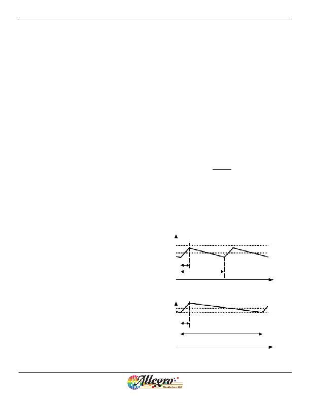
�Figure� 1� illustrates� how� the� current� is� limited� during� an� overload�
�condition.� The� current� decay� (period� with� switch� off)� is� propor-�
�tional� to� the� output� voltage.� As� the� overload� is� increased,� the� out-�
�put� voltage� tends� to� decrease� and� the� switching� period� increases.�
�VIN1� and� VIN2� VIN1 is a high voltage input, designed to with� -�
�stand 50 V. Bulk capacitance of at least 10 μF should be used to �
�decouple input supply VIN1. The VIN2 input is used to supply �
�the� linear� regulator� and� should� be� connected� directly� to� the� output�
�of the switching regulator when the target for the V� SW� voltage� is�
�between 3 and 5.5 V. For voltages outside of that range, the bias �
�supply for the IC is taken from VIN1 directly and affects overall �
�efficiency.�
�For applications where the switcher voltage is greater than 5 V, a �
�second supply between 3 and 5.5 V can be used to supply VIN2 �
�bias� current� and� the� linear� regulator.� Note� that� the� current� into� the�
�VIN2 supply must supply both the i� dd� bias� current� and� any� cur-�
�rent� load� on� the� linear� regulator.�
�Output� Voltage� Selection� The� output� voltage� on� each� of� the�
�two� regulators� is� set� by� a� voltage� divider� off� the� regulator� output,�
�as� follows:�
�R2� ?�
�?� ?�
�?� (2)�
�?� ?�
�In� order� to� maintain� accuracy� on� the� regulators� the� equivalent�
�impedance� on� the� FB� node� (R1� parallel� with� R2)� should� be�
�approximately 10 k?.�
�Inductor� current� operating� at� maximum� load�
�Current� Limit� level�
�Maximum� load�
�Constant� On-Time�
�Constant� period�
�Time�
�Inductor� current� operating� in� a� “soft”� overload�
�Overload�
�Current� Limit� level�
�Constant� On-Time�
�Extended� period�
�Time�
�Figure� 1.� Current� limiting� during� overload�
�Allegro� MicroSystems,� LLC�
�115� Northeast� Cutoff�
�Worcester,� Massachusetts� 01615-0036� U.S.A.�
�1.508.853.5000;� www.allegromicro.com�
�8�
�发布紧急采购,3分钟左右您将得到回复。
相关PDF资料
APP-001-15AMP
PLUG AUTO PWR BLACK W/LED 15AMP
APP-001-20AMP
AUTO PLUG 12VOLT WITH 20AMP FUSE
APP-001-VO
PLUG AUTO PWR BLACK W/LED IND
APP-001
PLUG AUTO PWR BLACK W/LED IND
APP-002
PLUG AUTO PWR GRAY W/LED IND
APP-003
PLUG AUTO PWR BLACK W/O LED IND
APP-004
PLUG AUTO PWR GREY
ARD00386
BOARD MCP1640 2CELL BOOST CONV
相关代理商/技术参数
APEK4403GEU-01-T
制造商:Allegro MicroSystems 功能描述:PRODUCT EVALUATION KIT
APEK4403GEU-01-T-DK
功能描述:BOARD EVAL FOR A4403 RoHS:是 类别:编程器,开发系统 >> 评估板 - DC/DC 与 AC/DC(离线)SMPS 系列:- 标准包装:1 系列:- 主要目的:DC/DC,步降 输出及类型:1,非隔离 功率 - 输出:- 输出电压:3.3V 电流 - 输出:3A 输入电压:4.5 V ~ 28 V 稳压器拓扑结构:降压 频率 - 开关:250kHz 板类型:完全填充 已供物品:板 已用 IC / 零件:L7981 其它名称:497-12113STEVAL-ISA094V1-ND
APEK4447SLJ-01-T-DK
功能描述:A4447 - DC/DC, Step Down 1, Non-Isolated Outputs Evaluation Board 制造商:allegro microsystems, llc 系列:- 零件状态:有效 主要用途:DC/DC,步降 输出和类型:1,非隔离 功率 - 输出:- 电压 - 输出:0.8 V ~ 24 V 电流 - 输出:2A 电压 - 输入:8 V ~ 50 V 稳压器拓扑:降压 频率 - 开关:- 板类型:完全填充 所含物品:板 使用的 IC/零件:A4447 标准包装:1
APEK4490EES-01-T-DK
功能描述:BOARD EVAL FOR A4490 RoHS:是 类别:编程器,开发系统 >> 评估板 - DC/DC 与 AC/DC(离线)SMPS 系列:- 标准包装:1 系列:- 主要目的:DC/DC,步降 输出及类型:1,非隔离 功率 - 输出:- 输出电压:3.3V 电流 - 输出:3A 输入电压:4.5 V ~ 28 V 稳压器拓扑结构:降压 频率 - 开关:250kHz 板类型:完全填充 已供物品:板 已用 IC / 零件:L7981 其它名称:497-12113STEVAL-ISA094V1-ND
APEK4491EES-01-T-DK
功能描述:A4491 - DC/DC, Step Down 3, Non-Isolated Outputs Evaluation Board 制造商:allegro microsystems, llc 系列:- 零件状态:有效 主要用途:DC/DC,步降 输出和类型:3,非隔离 功率 - 输出:- 电压 - 输出:- 电流 - 输出:- 电压 - 输入:4.5 V ~ 23 V 稳压器拓扑:降压 频率 - 开关:550kHz 板类型:完全填充 所含物品:板 使用的 IC/零件:A4491 标准包装:1
APEK4900KLQ-01-T-DK
功能描述:A4900 - Power Management, Half H-Bridge Driver (External FET) Evaluation Board 制造商:allegro microsystems, llc 系列:- 零件状态:过期 主要用途:电源管理,半 H 桥驱动器(外部 FET) 嵌入式:- 使用的 IC/零件:A4900 主要属性:3 个半 H 桥驱动器 辅助属性:- 所含物品:板 标准包装:1
APEK4910KJP-01-T-DK
功能描述:A4910 - Power Management, Half H-Bridge Driver (External FET) Evaluation Board 制造商:allegro microsystems, llc 系列:- 零件状态:有效 主要用途:电源管理,半 H 桥驱动器(外部 FET) 嵌入式:- 使用的 IC/零件:A4910 主要属性:3 个半 H 桥驱动器 辅助属性:- 所含物品:板 标准包装:1
APEK4915MET-01-T DK
制造商:Allegro MicroSystems LLC 功能描述:BOARD DEMO FOR 4915